Product

1. World-class Japanese brand, quality No.1
2. High measurement stability and reproducibility
3. High wear resistance and long life
Brand: Olympus
Model: Many styles, please refer to the attachment and link information
The ideally vertical side walls of the chip have two remarkable features
1) Ease in chip handling
Vertical side walls provide larger contact area to grab the chip by tweezers compared with conventional trapezoidal chip cross section. You can grab the chip by tweezers with stability, and avoid the loss of chip by bungled handling. The “New Concept Chip” can save your chip cost.
2) Eliminate problems with chipping and debris
Product features
Category of OLYMPUS micro cantilevers
1. Silicon cantilever for AC mode
TipView Design : for exact probe positioning
New Concept Chip : easy to handle with tweezers
Low Resistive Silicon : for anti-electrostatic charge
2. Silicon Nitride cantilever
Superior Durability and Small Spring Constant
Suitable for Contact mode and AC mode in water
3. Cantilever for Biological Sample Measurements in Water
Nanoscale Measurement
Force Curve Measurement
Observing Dynamic Behavior of Bio Sample in water
New Concept Chip
TipView
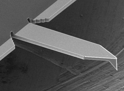
The tip is located on the very end of the cantilever. This feature allows you to set the tip over a point of interest on the sample, easily and precisely,
if you use an AFM combined with an optical microscope.
Measurement example
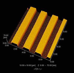
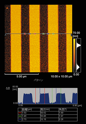
Measurement example (1) 50nm difference on wafer
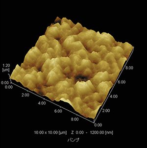
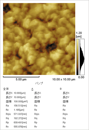
Measurement example (2) wafer bump
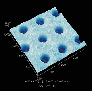
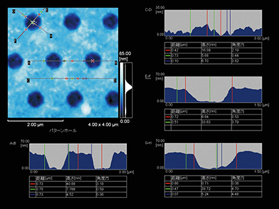
Measurement example (3) IC pattern hall

.GIF)