Main feature:
1. Large size scan ----- can measure the largest sample to 12 inches
2. Programmable electric control sample stage
3. The highest cost performance
4. High rigidity design and anti-vibration system----easy measurement at any time and place
5. Get nanometer surface features quickly and accurately-you can get high-resolution images in five minutes
Purpose:
Provide three-dimensional surface morphology images, including surface roughness, particle size, height difference and spacing
Brand: FSM
Model: LS-AFM
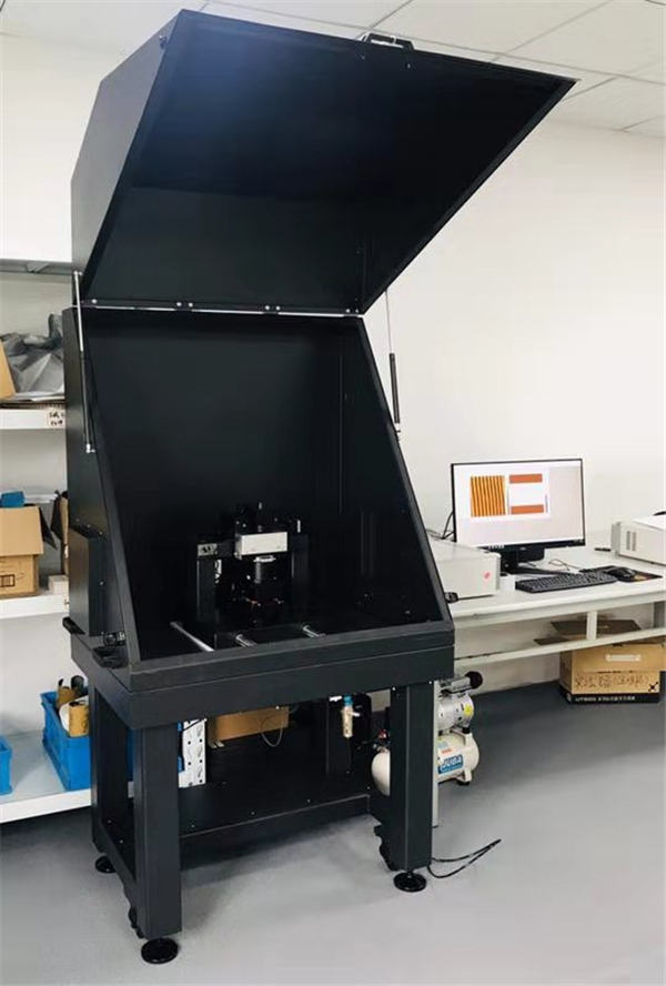
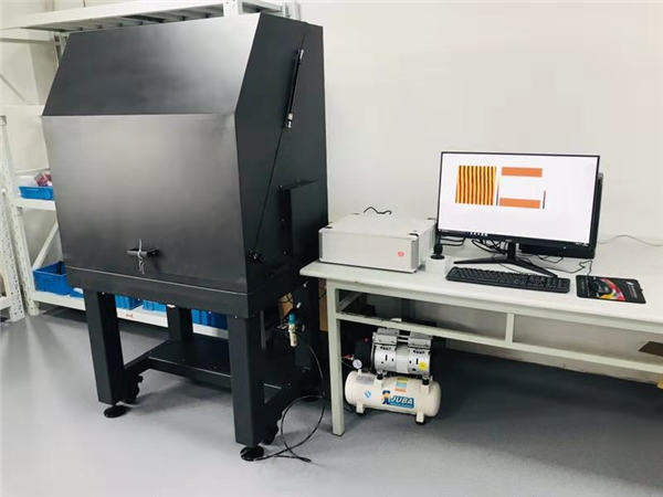
Product

Industrial AFM
Overview
The most intuitive, fast and cost-effective industrial AFM,
4”-12” samples can be tested directly on the machine without damage,
Set the coordinate automatic positioning, so that you can easily measure,
The best weapon for product development and quality control!
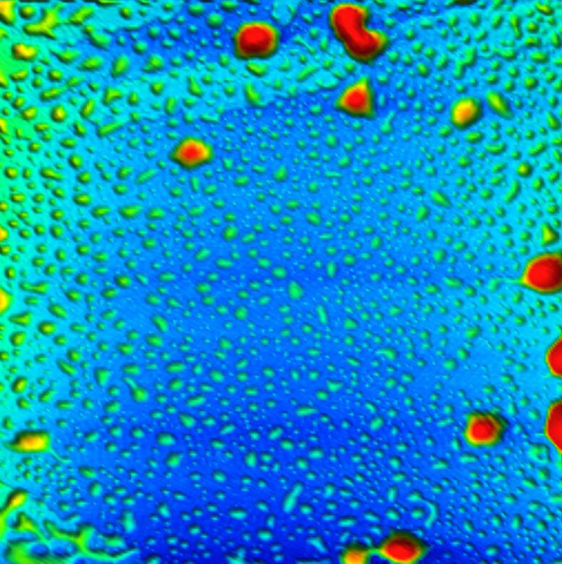 Alumina Al₂O₃
 STO film
 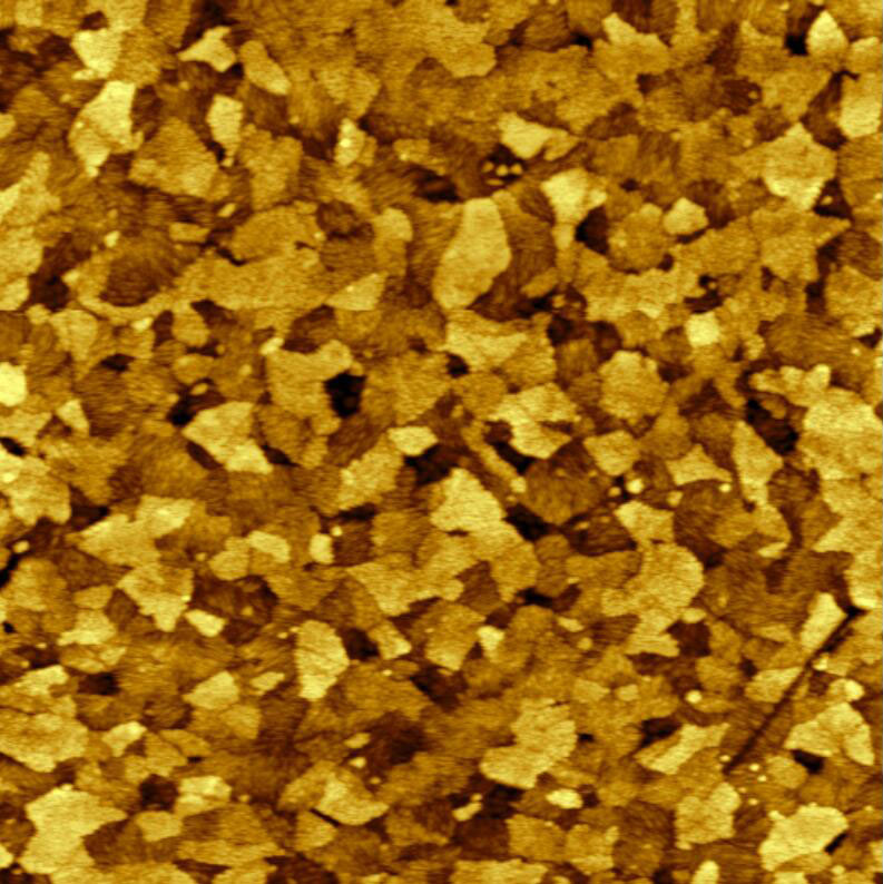 ITO film
Features:
1. Provide 6-inch or 12-inch sample measurement without sample weight limitation.
2. Ultra-long travel two-dimensional electric sample moving table, quickly input the coordinates for the position to be measured and then automatically position the lower needle.
3. Gantry scanner design, with marble base and vacuum adsorption stage.
4. Motor control and piezoelectric ceramic scanner automatically detect the needle feeding method, effectively protect the probe and sample.
5. Automatic optical positioning, no need to adjust the focus, observe and locate the probe sample scanning area at any time.
6. The most cost-effective industrial AFM with large stage
Applications:
1. Evaluate the difference before and after wafer processing (SiO2, GaAs, SiGe, etc.)
2. Determine the treatment effect of biomedical equipment (eg plasma treatment), such as contact lenses, catheters and coated stents
3. Check the effect of surface roughness on adhesion
4. Evaluate the groove shape and cleanliness of the patterned wafer
Analysis cases:
1. Coating analysis: roughness analysis, film thickness analysis, hole size analysis
2. Nano material analysis: particle size analysis, dispersion analysis
3. The surface structure can be converted into 3D images, which can quickly solve the material structure and morphology.
4. Material surface elasticity distribution, frictional force distribution, charge distribution, magnetic area distribution analysis, etc.
Technical Specifications
Specifications:
Basic mode: Tapping, Contact. Options: Phase, MFM, EFM, LFM
Scan rate: 0.6Hz~4.34Hz
Force graph curve: F-Z curve, RMS-Z curve
Scanning angle: 0~360°
Optional mode: Profile line fast measurement mode
Operating system: Windows XP/7/8/10 operating system
Scanning range: XY: 50um, Z: 5um
Communication method: USB2.0/3.0
Scanner resolution: XY: 0.2nm, Z: 0.05nm
Shockproof design: air-floating shockproof table/metal soundproof box
Sample size: Φ=150mm (6 inches), 300mm (12 inches), H<20mm
Equipment size: 800×600×500mm
Equipment weight: 150Kg
Sample moving range: 300×300mm
Optical microscope specifications 10X objective lens/1um resolution