Main feature:
1. Quickly and accurately obtain nano-surface features-high-resolution images can be obtained within five minutes
2. Intuitive operation and quick start --- less than 5 minutes from starting to scanning
3. The most cost-effective --- the price of other brands sold on the market is less than 1/2 (NTD can be owned within 1 million)
4. High rigidity design and anti-vibration system ---- easy measurement at any time and place
5. Designated and approved by the first-level research unit
Purpose:
Provide three-dimensional surface morphology images, including surface roughness, particle size, height difference and spacing
Brand: FSM
Model: Nanoview1000, Nanoview2000
Product

Research AFM
Overview
Beginners can complete all the settings within three minutes, about 5-10 minutes to get a high-resolution image that can be placed on paper, Many first-level research institude are designated for use.
Four characteristics:
1. Excellent efficiency, high stability.
2. High isolation performance, and no need to purchase additional optical isolation table, can be tested at any time and place.
3. The operation is extremely convenient, and the machine is quickly operated without the need for special maintenance.
4. The price is extremely affordable for everyone and every labs.
5. The liquid module, atmosphere and temperature control module can also be extend option.
How it works:
The probe is composed of a needle tip attached to the front end of a crossbar. When the probe tip is in contact with the surface of the sample, the elasticity of the crossbar is equivalent to the force between the atoms. The force will move the bar in the direction of the vertical force. The source of force includes the Van der Waals force of the probe and the surface and the Coulomb repulsive force between the probe and the outer electrons of the surface..
Therefore, the fluctuation of the surface of the sample causes the horizontal bar to shift up and down. Piezoelectric scanner with three-axis displacement capability enables the sample to scan back and forth in the selected area and detect the offset of the bar. The feedback circuit of the system and the piezoelectric material scanner are on the height axis The upper distance fine-tuning function is combined to maintain the fixed atoms during the scanning process by adjusting the distance between the probe and the sample, so when AFM scans an area, the vertical fine-tuning distance is stored as a two-dimensional internal function to form the so-called scanning area. Atomic force images, which usually correspond to the image of the high and low fluctuations of the surface of the scanning area, also known as height images.
Applications:
1. Evaluate the difference before and after wafer processing (SiO2, GaAs, SiGe, etc.)
2. Determine the treatment effect of biomedical equipment (eg plasma treatment), such as contact lenses, catheters and coated stents
3. Check the effect of surface roughness on adhesion
4. Evaluate the groove shape and cleanliness of the patterned wafer
Analysis items:
1. Coating analysis: roughness analysis, film thickness analysis, hole size analysis
2. Nano material analysis: particle size analysis, dispersion analysis
3. The surface structure can be converted into 3D images, which can quickly solve the material structure and morphology.
4. Material surface elasticity distribution, frictional force distribution, charge distribution, magnetic area distribution analysis, etc.
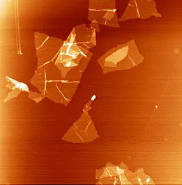
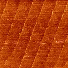
Actual test results
 |
 |
 |
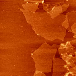 |
Graphene and graphite steps
Technical Specifications
Standard working mode: Contact mode (contact mode), Tapping mode (tap/half contact mode)
Optional modes: LFM mode friction/lateral force, Phase mode amplitude/phase, MFM mode magnetic force and EFM mode electrostatic force distribution measurement
Accessories selection: liquid module, temperature control module, atmosphere module
Sample size: Φ≤90mm, H≤20mm
Scanning range: XY to 20um, Z to 2um (additionally optional or additional scanners of XY to 10um, 50um or 100um, Z to 1um, 5um or 10um)
Scanning resolution: XY to 0.2nm, Z to 0.05nm
Sample moving range: 0~13mm
Optical magnification 4X, optical resolution 2.5um
Scanning speed: 0.6Hz~4.34Hz, scanning angle 0~360°
Scanning control: XY uses 18-bit D/A, Z uses 16-bit D/A
Attached high-efficiency suspension shockproof system
With moisture-proof and soundproof box